


TF Electronic Components Ultilize International Manufacturing Standards, AQL Sampling Plans, and Grid Inspector Training, Continuous Reseach and Experimentation by Our Quality Control Team has Generated Creative Solutions to the ever-Evolving Technologies Utilized to Mask Counterfeit Electronic Components, This Proactive Dedication Keeps TF Electronic and Our Clients Ahead of Market Attempts to mask the true condition of Components, All Processesare Conducted by TF Electronic Components.
Visual Inspection X-Ray Analysis Decapsulation Analysis Resurfaced Top-Side
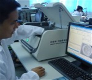
Spectrometer Dimension Verification High-Magnification Inspection Wafer Art
Resurfaced Part Refurbished Substrate Re-Balled BGA Counterfeit Labels
Lead frame profiles can vary but may not be counterfeit Insufficient PTH Solder Fill Dummy Part
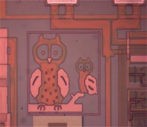
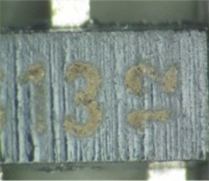
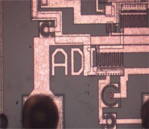
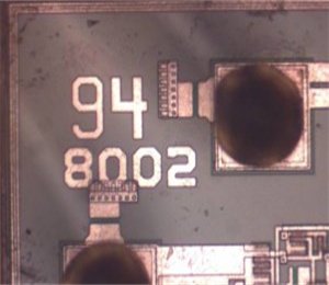
Marked MAX412 Analog Devices Die Marking 8002 Part Number Ahem…Wafer Art
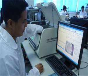
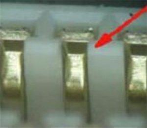
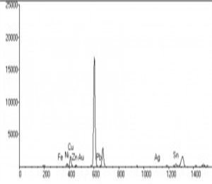
Fake Gold Connectors Copper not Gold-plated 67,923ppm Lead Content Spectrometer
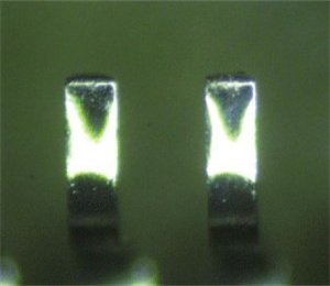
Leads Solder-Ability Pass Solder-Ability Fail BGA Solder-ability
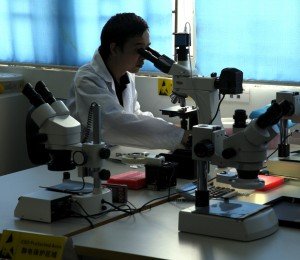
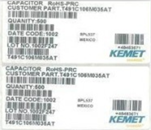
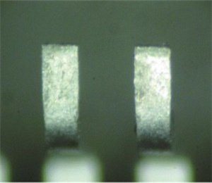
Using 3D microscope to test components from 360 degrees. Emphasis on checking outer packing condition, checking complete parts number, date code and lot code on the label; Chips marking and body condition; terminal layout,coplanarity and electroplating status, etc.; check if dimensions of the chip is in accordance with the specification of the data-sheet, etc.
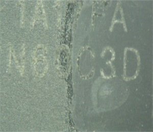
Use American army regulation chemical agent wipe the test object, to identify if this chips has been remarked or not.
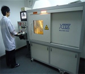
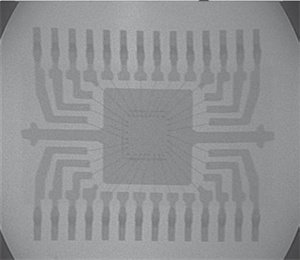
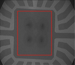
Use X-Rays to analysis the internal structure of chips. With X-ray detection, we can find out if the internal structure of test objects are consistent or they are mixed parts; Mixed parts means there are different size wafer, different base,different wire frame, different line up from the same batch products, etc.; In addition, it also can intuitively see the internal wire of chips open / short circuit, these defective will directly cause the product function failure.
Check the X-Ray image of test object according to the Pin definition on original data-sheet, identify if the chips Pin definition is consistent.
Take out the die with chip anatomical methods, analysis the die logo, wire, structure, MASK etc, to identify whether the chips are from original factory.
Use of VLSI/SOC test system, its diversified test function can be applied to display IC, LEDIC, power IC, digital consumption IC, CSTN, OLED, MCU and peripheral devices of IC etc, testing center provides the most economical production testing and comprehensive test plan, provide complete Socket to meet various needs of packaging.